You are currently viewing only those items made visible to the public. Click here to sign in and view the full catalogue.

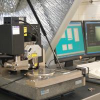
Dimension 3100 AFM
| MANUFACTURER | Bruker |
|---|---|
| MODEL | 3100 AFM |
| ACRONYM | AFM |
| AVAILABILITY | 8am to 6pm. Evening and weekend use by experienced users only |
|---|---|
| RESTRICTIONS | None |
| TRAINING | Training is required to use this item and we can arrange this if needed. |
| CONTACT 1 | Richard Thorogate |
|---|---|
| CONTACT 2 | Bart Hoogenboom |
| Enquire about this item | |
| SITE | Bloomsbury Campus |
Description
The Dimension 3100 utilises standard and advanced SPM imaging modes for measuring semiconductor wafers, lithography masks, magnetic media, biomaterials, optics and other materials. The sample stage will allow large sample sizes (up to a 6 inch wafer) with a scan size up to 100 µm in the X & Y and 6 µm in the Z.
Specification
Contact mode Tapping mode Phase imaging Lateral force mode Force imaging MFM Electric techniques (CAFM, Tuna) Closed loop option
Item ID #.
Last Updated: 6th November, 2015
There are no publically available categories listed at present. You may have to sign in to browse this catalogue.
